![]()
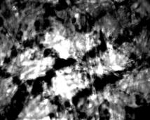
NIR microscope image of interior circuits of bonded silicon device

NIR microscope image of currency
The NIR microscope, also known as the SWIR microscope, is engineered to capture the intricate features of microscopic samples beyond the visible spectrum through absorbance, reflectance, fluorescence, and emission in the visible, near-infrared, and shortwave infrared regions. Optimized for superior performance in the NIR range, this advanced instrument offers a broad spectral range covering ultraviolet, visible, and NIR. Its non-destructive imaging capabilities make the NIR microscope indispensable for a variety of applications, revealing hidden details in microscopic samples without causing any damage.
Pharmaceutical & BiologyNIR Fluorescence of Biological Samples
Pharmaceutical Quality Control
Active Ingredient Dispersal Imaging
Contaminant Analysis
Cellular Imaging
Moisture Imaging
Semiconductor & DisplaysLocating Defects Within Bonded Silicon Wafer Devices
Quality Control of Diode Lasers
Materials Research
Carbon Nanotube Imaging
Microfluidic Device Development
Polymer Microimaging
GeologyMineral Imaging
Petroleum Analysis
Art & ForensicsImaging Reused Canvases
Security Imaging
And more...NIR Microscope Applications NIR Microscope Design UVM-1 NIR Microscope UV Microscope Applications UVM-1 UV Microscope NIR microscope image of interior circuits of bonded silicon device NIR microscope image of currency The NIR microscope is designed to image in regions beyond the visible range. While the usable spectral range of this microscope covers the ultraviolet, visible and NIR regions, their optics and light sources are optimized so that they are more effective in the NIR region. As such, there are many uses for NIR microscopes as they can non-destructively image microscopic samples in regions other than the visible. Pharmaceutical & Biology NIR Fluorescence of Biological SamplesPharmaceutical Quality ControlActive Ingredient Dispersal ImagingContaminant AnalysisCellular ImagingMoisture Imaging Semiconductor & Displays Locating Defects Within Bonded Silicon Wafer DevicesQuality Control of Diode LasersMaterials ResearchCarbon Nanotube ImagingMicrofluidic Device DevelopmentPolymer Microimaging Geology Mineral ImagingPetroleum Analysis Art & Forensics Imaging Reused CanvasesSecurity Imaging And more...

